
Reliably complete solar cell inspections
Quality assurance in the production of wafers
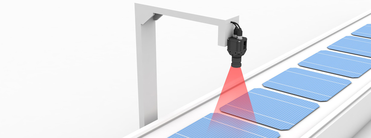
The manufacturing process of solar cells creates several layers, including front and rear electrodes, a silicon layer and a structured surface with an anti-reflective coating. Cracks, scratches, inclusions or other defects can have a significant negative impact on the function and efficiency of the solar cell and need to be detected at an early stage. This makes inspection a crucial step in the production of PV cells.
Our SWIR image sensors (Short Wave InfraRed) open up application possibilities in frequency ranges beyond visible light at wavelengths of up to 1700 nm. Silicon becomes transparent in SWIR light, making it particularly easy to inspect structures in the wafers.

Industrial cameras are used in a variety of applications in the semiconductor industry, including automatic optical inspection (AOI). Our industrial cameras deliver high-resolution, low-noise images with a high dynamic range. This makes it possible, for example, to identify defects such as scratches, damage, particles, and so forth, with exceptional reliability during wafer inspection or to verify critical dimensions during wafer metrology
Benjamin Renz, Global Market Segment Manager, Semiconductors & Electronics
Features
- Uses state-of-the-art CMOS image sensors
- Rolling shutter or global shutter with back side illumination, suitable for the most difficult lighting conditions
- Reduced computing power required thanks to data pre-processing on FPGA in the camera
- Individual customization to the application is possible
Products for wafer inspection
We can help you get the best out of your systems
Downloads
-
Industry brochure semiconductor industry
-
Custom Design and Engineering – custom specific camera and sensor solutions
-
Industrial cameras with SWIR and UV sensors