
From Binary Basics to Semiconductors: Understanding the Building Blocks of Modern Electronics
On the most basic level, electronic communication relies on a binary interface consisting of 0s (off) and 1s (on).
Reading Time: minutes
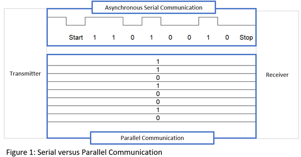
Initially, this blog was intended to focus on serial communications used for IO-Link. In essence, serial communication involves transmitting binary data either asynchronously (without a clock) or synchronously (with a clock). Figure 1 is an oversimplified comparison of serial transmission versus parallel transmission. The goal was to show the differences and similarities that IO-Link shares with other serial communications, such as RS-485 or RS-232. However, before diving into serial communications, it’s important first to understand the fundamentals of binary principles.
On the most basic level, electronic communication relies on a binary interface consisting of 0s (off) and 1s (on). While transistors can function as amplifiers, for simplicity, we’ll consider them as switches that toggle between off or on states.
 In electronics, materials are classified into the following three groups based on their electrical properties:
Conductors, such as copper, silver, aluminum, and gold, readily allow electrical current to flow.
Insulators, like glass, plastics, and wood, block electrical current under normal conditions.
Semiconductors, such as silicon (Si), germanium (Ge), and carbon (C), can conduct electricity but require an external voltage to do so.
In this discussion, I will focus on the semiconductor group.
The PN-junction is formed by combining two types of semiconductor materials: N-types and P-types. Silicon, the most common semiconductor, starts in an intrinsic state, meaning it is neither P- nor N-type by default. Impurities are added through the process of “doping” to transform silicon into a P-type or N-type.
N-type semiconductor:
The “N” stands for negative (-) charges or electrons.
Electrons are the majority carriers.
Holes (positive charges) are the minority carriers.
N-type semiconductors can donate electrons.
Common elements used for doping include phosphorous (P), arsenic (As), antimony (Sb), and bismuth (Bi).
P-type semiconductor:
The “P” stands for positive (+) charges or holes.
Holes are the majority carriers.
Electrons (negative charges) are the minority carriers.
P-type semiconductors can accept electrons.
Common elements used for doping include aluminum (Al), gallium, boron, and indium (In)
PN-junctions are important in many fundamental electronic components, including diodes, silicon-controlled rectifiers (SCRs), programmable unijunction transistors (PUTs), and transistors (both bipolar junction and field-effect types). In this discussion, I will focus on transistors, the basic means for creating and interpreting 0s and 1s.
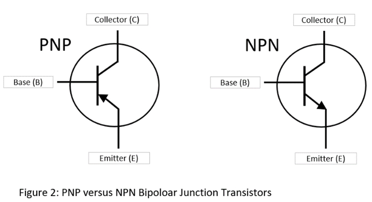
The doping process determines whether a transistor is a PNP or NPN type. Bipolar junction transistors consist of three connections: the base (B), collector (C), and emitter (E). Figure 2 shows the electronic symbols PNP and NPN transistors.
 Field-effect transistors (FETs) use a similar nomenclature but have different terminal names: gate (G), drain (D), and source (S).
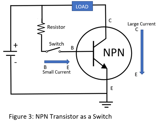
Figure 3 shows how an NPN transistor operates as a switch. When the base is forward-biased –meaning a voltage is applied between the base and emitter (closing the switch) –the transistor turns on, allowing current to flow from between the collector and emitter or from the load to the ground. This basic concept is widely applied throughout electronics.
 While understanding the physical composition of transistors isn’t essential for grasping the concept of 0s and 1s, it is still cool to know. The main takeaway is recognizing how transistors function and how semiconductors drive the advancement of digital technology.
The main reason processors have become faster is largely due to semiconductor manufacturers fitting billions of transistors into a single chip. It is difficult even to comprehend that a transistor can be as small as 10 nanometers (0.00000001 meters). While knowing this won’t help you decode the Matrix, you should at least understand that binary code works by turning various pathways on and off to reach the desired location or outcome.

Popular posts
Industrial sensing fundamentals – NPN vs PNP
What is a capacitive sensor?
How do I wire my 3-wire sensors?
The basic operating principle of an inductive proximity sensor
Contact form
Do you have any questions or suggestions? We are at your disposal.
Balluff Inc.
-
8125 Holton Dr.
Florence, KY 41042