
Enhancing Semiconductor Manufacturing With RFID
RFID automates real-time tracking in semiconductor manufacturing, enhancing precision and efficiency

Reading Time: minutes
The semiconductor industry requires precision. With thousands of wafers in production at any given time, real-time visibility into processes, materials, and assets is essential. Yet, many fabs still use outdated tracking methods that create inefficiencies and risks. RFID is changing the industry by enabling automation and accurate and scalable tracking for semiconductor manufacturing.
The visibility problem in semiconductor fabs
Tracking is critical in a semiconductor fab. Wafers must move through hundreds of tightly controlled steps; raw materials must meet strict compliance standards; and high-value tools must always be in the right place at the right time. The stakes are high, and mistakes are costly.
Traditional tracking methods such as barcodes, manual data entry, or spreadsheets create blind spots and increase the risk of human error. Misplaced wafer carriers can stall production, expired chemicals can compromise yield, and inefficient tool usage can cause unnecessary downtime. FID offers a smarter, more reliable solution.
RFID’s role in semiconductor manufacturing
RFID transforms semiconductor tracking by providing real-time, automated visibility. Unlike barcodes, it works without direct line-of-sight, making it ideal for high-speed, high-precision environments.
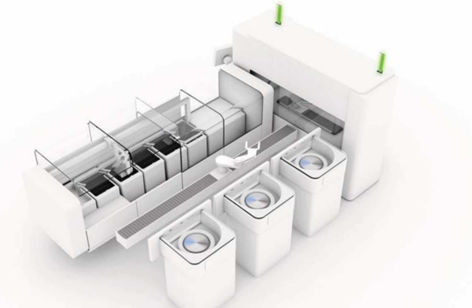
Wafer carrier tracking (FOUPs and FOSBs)
In a semiconductor fab, every wafer travels in a Front Opening Unified Pod (FOUP) or Front Opening Shipping Box (FOSB), which must be traceable at every step.
How it works: RFID tags on wafer carriers allow for automated identification as they move through tools, storage, and transport systems.
Benefits: It eliminates manual scanning, reduces handling errors, and optimizes workflow efficiency.
 Material tracking: chemicals and raw wafers
Semiconductor production relies on controlled materials such as photoresists, etchants, and gases, which must be used precisely and within their expiration limits.
How it works: RFID tags track each chemical batch, logging when and where materials are used.
Benefits: The system ensures compliance with safety regulations, prevents material waste, and enhances inventory management.
Finished goods tracking
Traceability continues even after wafers are transformed into semiconductor chips. RFID technology extends to packaging and distribution.
How it works: RFID tags are attached to finished goods to track them during storage and shipping.
Benefits: RFID improves logistics visibility, reduces the risk of counterfeiting, and enhances customer service by providing accurate delivery tracking.
Asset management: keeping tools in the right place
Semiconductor fabs rely on precision tools, from photolithography machines to test equipment, requiring strict tracking and maintenance schedules.
How it works: RFID tags on tools automate usage tracking and maintenance logs.
Benefits: They reduce tool misplacement, optimize asset utilization, and prevent unplanned downtime.
Process monitoring: controlling the fab environment
A single variation in temperature or humidity can affect semiconductor yield. RFID supports environmental monitoring within production areas.
How it works: RFID sensors track process parameters in real time, ensuring conditions stay within the required tolerance.
Benefits: RFID helps maintain product quality, ensures compliance, and reduces the risk of defects.
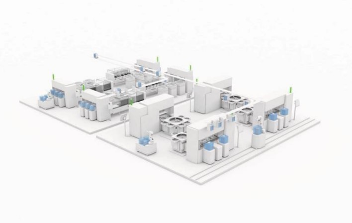 RFID and AGVs: smarter material handling
Automated Guided Vehicles (AGVs) are a staple in modern fabs, moving materials without human intervention. RFID enhances their efficiency.
How it works: RFID tags provide precise location data, guiding AGVs through complex production layouts.
Benefits: RFID minimizes transport errors, improves speed, and supports just-in-time material flow.
 Semicon-specific RFID solutions
While standard RFID solutions significantly enhance traceability in semiconductor fabs, some applications demand customized RFID systems to meet stringent operational and environmental constraints such as high-temperature processing, chemical exposure, and RF signal interference.
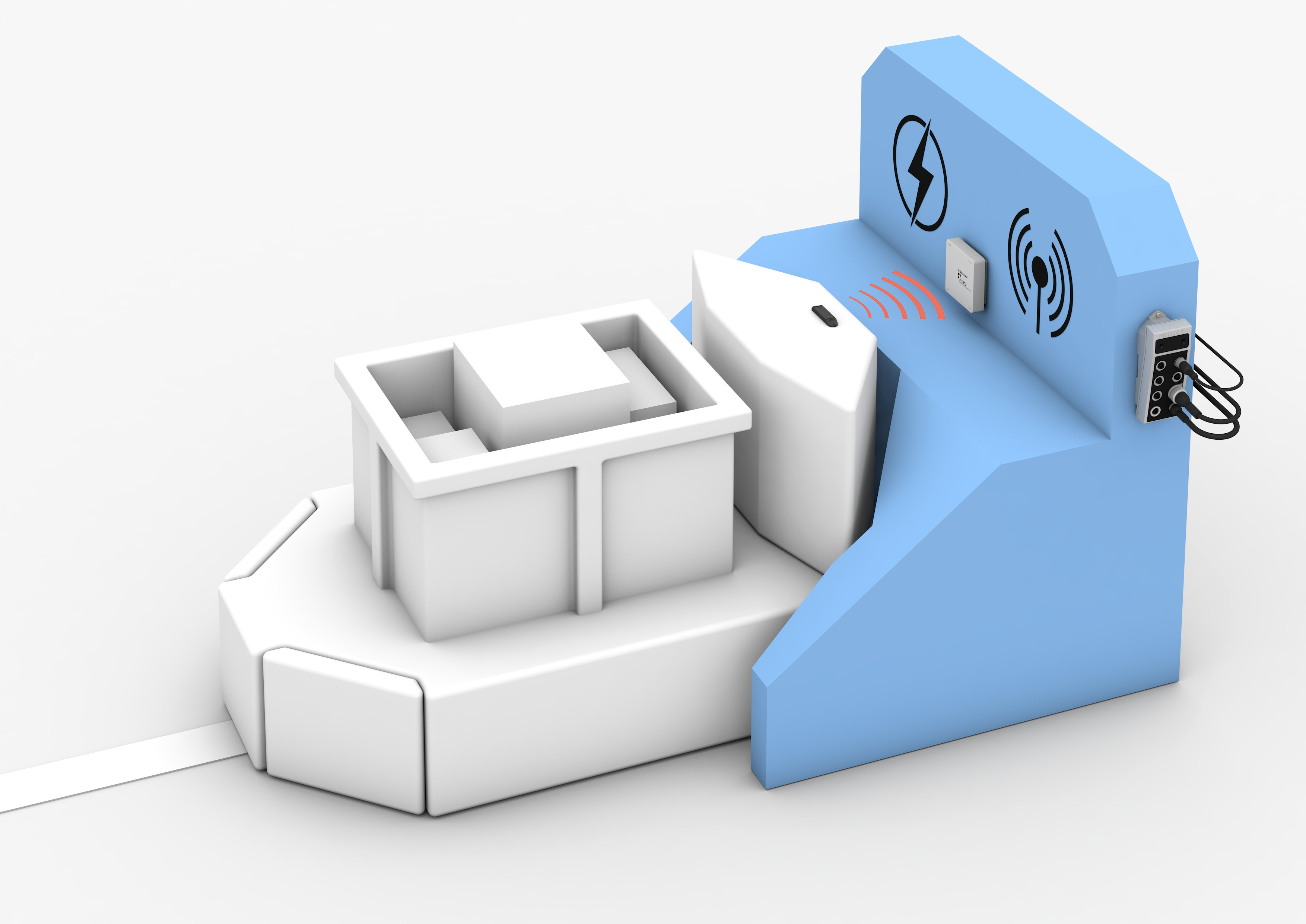
Why 134.4 kHz for semiconductor applications?
Interference-free performance: Low frequency (LF) RFID operates at a lower frequency, making it more resistant to interference from metal surfaces,
High reliability in harsh conditions: LF RFID tags are designed to withstand extreme temperatures, chemicals, and plasma environments, ensuring long-term durability in cleanrooms and chemical-processing areas.
Wafer carrier identification in high-density storage
o LF RFID enables precise tracking of FOUPs and FOSBs in dense storage environments, where metal racks can cause signal interference with other RFID frequencies.
o It ensures accurate FOUP identification at load ports without cross-scanning errors.
Why RFID is the future of semiconductor tracking
As the industry moves towards fully automated manufacturing, RFID will integrate with Manufacturing Execution Systems, AI-driven analytics, and IoT platforms to create self-optimizing production environments.
The fabs that succeed in the coming years will eliminate manual tracking, reduce inefficiencies, and embrace real-time data-driven decision-making. RFID is not just an upgrade. It is becoming the foundation of modern semiconductor manufacturing.
Keywords
- RFID
- Semiconductors
Author

Rob Kline
As product marketing manager for traceability at Balluff, Rob brings over 15 years of experience in factory automation, technical sales, and marketing. He‘s an expert in the fields of RFID and optical code reading. Before joining Balluff, this professional solved traceability problems at key market players in the vision and code reading industry. He brings deep technical knowledge and a wide understanding of industry trends in manufacturing, logistics, packaging, and life sciences.
27 Contributions