
OEM Customization Challenges: How Engineering Teams Solve Them Efficiently
A structured approach to customization in semiconductor and life science applications
Reading Time: minutes
Customization projects for large OEMs are rarely straightforward. Engineering teams must balance strict specifications, regulatory requirements and cost constraints, often under high time pressure.
This article explains how to approach OEM customization systematically and reduce technical risks.
Key Insights
OEM customization requires structured requirements, validation, and scalable design
Key challenges: “copy exact”, supply chain risks, and cost pressure
Modular design and early collaboration reduce complexity and risk
What Is OEM Customization?
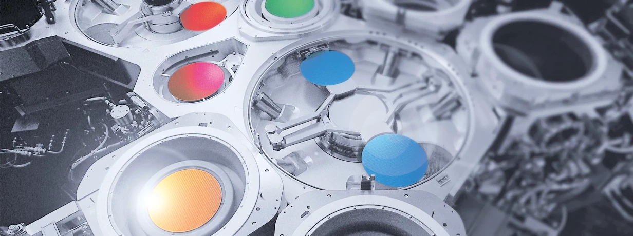
In semiconductors, engineers build sensors and vision systems that work in cleanrooms, move wafers quickly, and detect tiny defects. For example, wafer sensors need special materials and settings to work in vacuum chambers, while vision systems need clear lenses to find small faults.
In life sciences, R&D teams design sensors and devices that meet strict hygiene and safety rules. These products must handle liquids well, be traceable, and fit into clean lab environments. Engineers often use safe materials, make devices smaller, and connect them to lab automation.
Customization means changing standard products (like sensors, RFID, or vision systems) or making brand new designs to fit special needs. The big challenge for engineers is to balance what can be built, how easy it is to make, and if it meets the rules.
 Easy Steps for Customizing Products
Collect Requirements: Engineers need to talk with OEM partners to understand exactly what is needed—performance, environment, and rules. For example, a semiconductor sensor may need to work in a cleanroom, in a vacuum, and fit with current systems. In life science, needs may include safe materials and tracking for clean labs.
Check Feasibility and Design: Do careful study of the product, see what needs to be changed, and make sure the materials work. Engineers should look for risks, costs, and if they can be made easily. Adding a safe coating to a sensor, for example, means testing how materials behave and affect the process.
Build and Test Prototypes: Make prototypes and test them in real conditions. Use modeling tools and repeat tests to make sure they work. For semiconductors, “copy exact” rules mean products must be calibrated and checked very carefully.
Validate Rules and Standards: Make sure designs meet industry standards like ISO 14644 for cleanrooms and ISO 13485 for medical devices. For life science products, tracking and contamination checks are important.
Plan for Production: Prepare for making the product on a scale. Find special materials and set up good process controls. Engineers should set strong quality checks to keep products consistent, especially for “copy exact” needs.
What are common Engineering Challenges?
Complex Contracts: Teams must work with contracts that have strict timelines and quality rules. Engineering leaders should push for clear schedules and open talk to reduce risks.
“Copy Exact” Requirements: Engineers must make sure changes match the original part’s performance. This needs careful testing, clear documents, and sometimes new tools for calibration.
Higher Specifications: OEMs want products that do more than usual—like sensors for extreme heat or safe for use in the body. Engineers must find new materials and make processes fit these needs, which makes things harder and costlier.
Supply Chain Issues: Custom products often need rare materials. Teams must work with buyers to find other sources, plan for delays, and keep the supply chain strong.
Cost vs. Innovation: R&D must deliver great solutions that don’t cost too much. Using modular designs, sharing R&D costs, and improving production can help balance new ideas and budgets.
 What does Supplier Reduction mean for Engineers?
OEMs want fewer suppliers with broader skills. Engineering teams need to develop skills across sensors, vision, and automation, learn new things, and show they can deliver in many areas. Having fewer suppliers makes integration easier but requires more scalability and quality.
Cost Efficiency: Engineering Tips
Use modular sensor systems for different OEM needs to save time and money.
Share development costs with OEMs, especially for risky projects.
Standardize processes and materials, buy in bulk, and improve quality control to lower costs.
Collaboration and Trust: Best Practices
Working closely with OEMs is key. Define requirements together, build prototypes side-by-side, and share risks. Trust comes from open talk, regular meetings, and always delivering on time. Engineers should keep all technical decisions documented and fix issues quickly.
How Can Engineering Teams Overcome Customization Challenges?
Build strong partnerships with OEMs: Start early, clarify what is needed, and review designs together.
Invest in flexible designs: Make modular, scalable platforms for many applications and easy customizations.
Improve supply chains: Find multiple sources, use digital tools for tracking, and keep extra stock of important materials.
Use advanced engineering: Simulate and test designs well before full production to reduce risks.
Negotiate fair contracts: Push for shared risks, realistic deadlines, and backup plans in agreements.
Conclusion
For engineering and R&D teams, customizing products for large OEMs in semiconductors and life science is a big technical challenge. It requires accuracy, new ideas, and good teamwork. By following clear steps, using the best tools, and building strong relationships, technical teams can solve customization problems and deliver products that help their industries succeed. As things change, great engineering—supported by digital tools and partnerships—will stay at the heart of industrial automation.
Keywords
- Industry 4.0
- Sensor technology
- Industrial automation
- Technology trends
- Smart sensor technology
- Life Science
- Inductive sensors
- Distance measurement
- Machine vision
Author

František Jakubec
Frank Jakubec, Head of Global Market Segment for Semicon & Electronics at Balluff, is a seasoned automation and technology specialist. With more than 15 yeards of experience in business-to-business product and solution sales, Frank is an expert in machine vision and has a talent for business development.
14 Contributions