06.09.2019
Mapping-Sensor – Delivering Precision in the Smallest Possible Space
Can be integrated into an end effector, ideal for wafer mapping
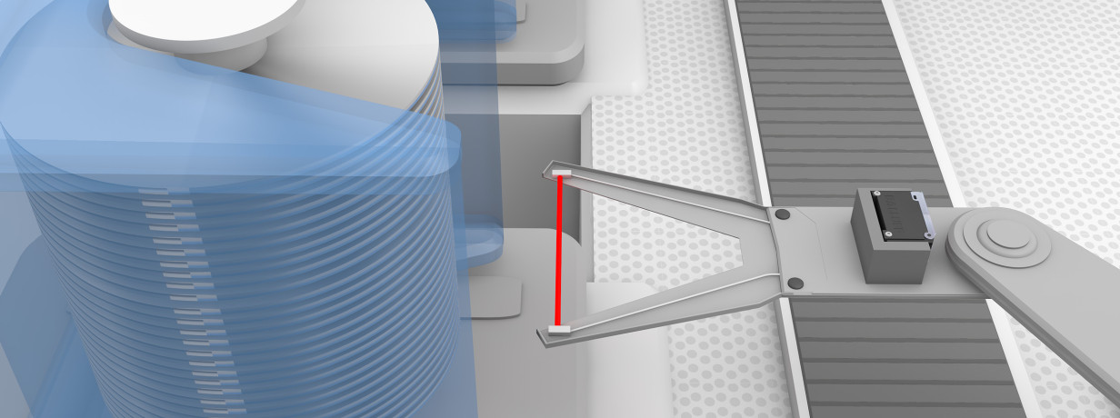
For your wafer mapping needs, Balluff offers a highly precise photoelectric sensor which integrates perfectly into an end effector. Especially designed for extremely thin end effectors, our mapping sensor features an extremely controlled and focused light spot with outstanding homogeneity. This allows the sensor to detect wafers even just a few μm thick with extreme precision. And you can be confident that it will reliably detect full slots, doubled wafers or tilted wafers will be reliably detected at all times.
The mapping sensor is based on the photoelectric Micromote technology, which combines an extremely small optical sensor head with an external processor unit (amplifier) and connects them via a highly flexible cable. This means you can adapt the mapping sensor to any mechanical installation situation, like other Micromote sensors.
Features
- Very compact, extremely flexible sensor cable
- Multi-functional sensor head
- Flexible adaptation to the respective application using an BAE external amplifier

Downloads
-
Mapping Sensor – delivering precision in the smallest possible space