
How UV and SWIR are Revolutionizing Industrial Vision Systems
When paired with the right lens, mounting, lighting, software, and processing, today’s industrial cameras form advanced imaging systems that play a key role in driving industrial intelligence.
Reading Time: minutes
The camera, invented nearly 200 years ago, took almost 130 years to find its way into manufacturing. By the mid-20th century, the first machine vision systems emerged, primarily designed for basic product inspections. Industrial inspection systems were transformed in the 1960s and 1970s with the advent of digital imaging. Although early cameras were large, had low resolution, and were costly, they paved the way for a shift from manual to automated vision systems. In the 1980s, charge-coupled device (CCD) image sensors and advanced software greatly improved industrial image processing, enabling cameras to tackle more complex tasks.
Today’s industrial cameras may still use CCD sensors, but complementary metal-oxide semiconductor (CMOS) image sensors are now preferred. CMOS sensors offer comparable image quality to CCDs while consuming less power, processing signals faster, and saving costs. When paired with the right lens, mounting, lighting, software, and processing, today’s industrial cameras form advanced imaging systems that play a key role in driving industrial intelligence.
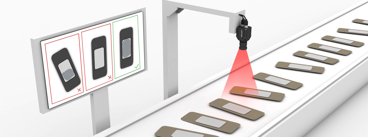
Expanding camera capabilities for complex manufacturing
Since their inception in 1826, most cameras have been designed to capture images within the visible light spectrum to portray an image as seen by the human eye faithfully. While they’ve effectively detected visible surface imperfections such as scratches, dents, or color inconsistencies, they were limited by their narrow (human) range of perception. As products and manufacturing processes became more intricate, the need for better insight into materials, surfaces, and components has grown.
Technological advancements in UV and SWIR imaging
Recent advancements in image sensor technology have introduced extended wavelength capabilities, allowing cameras to capture short-wave infrared (SWIR) and ultraviolet (UV) light. These innovations offer significant advantages by going beyond the visible spectrum. Industrial cameras with UV or SWIR CMOS image sensors can reveal hidden features, detect defects, and analyze material properties that are invisible to the human eye, opening up new possibilities in industrial applications, such as:
Seeing in ultraviolet (200 nm – 400 nm)
Defect detection – UV light, with shorter wavelengths, can penetrate smaller crevices than visible light, revealing additional image details.
Sorting – UV light interacts uniquely with different plastics, enabling sorting operations.
Fluorescence detection – By incorporating tracer materials into adhesives and lubricants, UV can detect leaks and excess fluids and verify proper coating during manufacturing processes.
Surface contamination - UV cameras can identify oils, chemical residues, and cleaning agents left on surfaces during manufacturing.
Microbial detection - Many microorganisms, including bacteria and fungi, naturally fluoresce under UV light. Others can be stained with UV-reactive dyes, enabling quick, high-resolution imaging of cultures or environmental samples.
Plasma excitation – UV cameras can detect photons emitted by excited plasma during vacuum/plasma semiconductor processes, generating images to help improve process control.
Seeing in short-wave infrared (400 nm – 1700 nm)
Moisture detection – SWIR cameras can penetrate deeper into materials, making them ideal for detecting moisture levels that affect product quality, particularly in industries like packaging, food and beverage, and paper production.
Internal defect detection – In automotive manufacturing, SWIR imaging can reveal internal defects, such as delaminations, voids, or structural inconsistencies in composites or metals.
Medical imaging – In the life sciences, SWIR imaging provides distinct advantages for biological research, medical diagnostics, and environmental monitoring by enabling the noninvasive visualization of biological tissues.
Monitor biological fluids – SWIR imaging is useful for monitoring biological fluids like blood and saliva, leveraging their absorption and scattering properties to identify biomarkers.
Wafer inspection – SWIR imaging is used in semiconductor manufacturing to detect defects in wafers and microchips, such as contamination, cracks, and structural imperfections that may not be visible with traditional optical inspection methods.
The integration of UV and SWIR capabilities in industrial cameras offers new insights into manufacturing processes. By capturing data beyond the visible spectrum, these advanced vision systems enhance real-time quality control, aid in predictive maintenance, and optimize processes.
Keywords
- Machine vision
- Machine Vision and Optical Identification
Author

Robert Crumley
20 Contributions